The Application Of 2D Materials For Research
It is very much essential to know what 2d materials are before using it in research work or before knowing the various kinds of it. The entire surface area is needed to build a 2D material. It is a distinct new material which possesses a thickness of one atom. The newly formed material is porous in nature and is quite flexible. This material is rigid and strong too. It falls in the category of Nanomaterials.
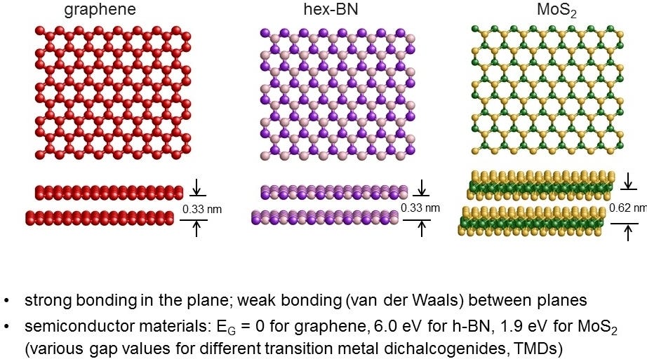
The two-dimensional plane allows the electrons to move freely. The commonly used 2d materials for research work are black phosphorus, graphene, dichalcogenides of a transition metal. These materials hold a crucial place for the scientists and the engineers. The reason behind this is the amazing properties they possess. These materials are also capable of improving in the devices that contain electron and photon.
The reason behind the use of 2d materials for research by the scientists
The diversity of 2d materials are just like the valleytronics, biosensing, electronics and catalyst and the application of it calls for the use of 2d materials for research. These materials help to gain a good amount of wealth. It is only concerned with layers of a single element, which may be graphene or phosphorene. The different properties of 2d materials help it to become valuable. These properties are – super electric conductor, great mobility carrier, mechanically flexible, superheat conductor, great optical strength and amazingly absorb ultra-violet rays of the sun.
The different kind of 2d materials used for research work
Silicone – It is rich in the electrical property that is derived from graphene and is one atom in thickness. This can be used in the making of small electronic devices and can also be used in the circuits which have a base made of silicon.
Boron – The material which is derived from nature and possess the texture of metal. It is mainly known for its conductivity to low temperatures. It has a great resisting power until the temperature falls down to 10 or 20 Kelvin, which is minus 430 degrees Fahrenheit.
Silica glass – If you ask for the thinnest glass then this is the one for you. It is made with the help of microscopy of the electron. It was discovered in Kavli Institute in New York by David Muller along with his colleagues.
We can conclude that the different 2d materials used in research work are rich in different properties which make them valuable and eligible for what it is used.


Comments
Post a Comment